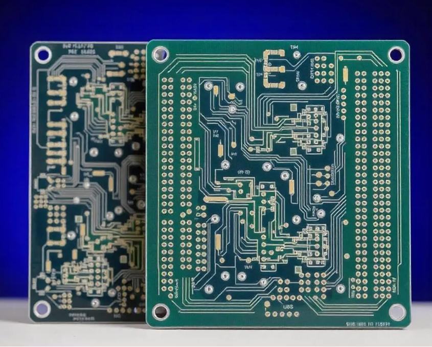
Two copper layers with plated through vias
Double sided PCBs allow signals and power to move between top and bottom copper layers, making them suitable for controllers, sensor boards, small IoT devices and many industrial modules.
XFPCB China PCB Manufacturer
A 2 layer PCB is the workhorse for many electronics projects: enough routing room for components on both sides, plated through holes for connection between layers, and a cost level that still fits prototype, low-volume and mid-volume production. XFPCB helps overseas buyers move from first Gerber review to repeat orders with clear engineering feedback, practical material options and dependable fabrication control.
Procurement intent
Most 2 layer PCB buyers need a supplier that can move quickly without treating the order as a blind upload. Procurement teams usually ask a deeper question: will this factory catch design risks before production and deliver double sided boards that are ready for assembly?
Double sided PCBs allow signals and power to move between top and bottom copper layers, making them suitable for controllers, sensor boards, small IoT devices and many industrial modules.
XFPCB can support early prototypes and then help stabilize the same part number for repeat production when the design becomes commercial.
We review drill size, annular ring, slot definition, via tenting, copper clearance and panelization before releasing the order.
Lead-free HASL, ENIG and OSP can be discussed according to soldering method, shelf-life requirement, pad flatness and cost target.
Manufacturing specification
For most 2 layer PCB projects, the RFQ should define the baseline board structure clearly. XFPCB confirms the manufacturing data before quoting so buyers can compare price, lead time and risk with more confidence.
| Specification | Common XFPCB options | Procurement note |
|---|---|---|
| Base material | FR-4 is the standard; high Tg can be considered when temperature or reliability demands increase | Material selection should match the product environment, not only the lowest prototype price. |
| Copper weight | Commonly 1 oz, with heavier copper reviewed by trace current and fabrication limits | High-current designs need wider traces, thermal relief review and clear copper notes. |
| Surface finish | Lead-free HASL, ENIG, OSP and other finishes by project requirement | ENIG helps pad flatness for fine pitch parts; HASL is often cost efficient for through-hole and standard SMT. |
| Mechanical details | Routed outline, V-score, slots, cutouts and panel rails | Incorrect slot or outline data is a common reason for delayed quotes and tooling questions. |
| Testing | Electrical test and visual inspection based on order requirement | A clear testing requirement helps protect assembly yield and incoming quality approval. |
Manufacturing review
A double sided PCB usually looks straightforward, but many first-time and repeat-order issues begin in small details: drill-to-pad clearance, plated slot definition, solder mask slivers, silkscreen over pads, insufficient copper relief, or a panel design that is difficult to depanel cleanly. XFPCB reviews these points so the buyer can correct risk before fabrication rather than after boards arrive.
For procurement teams working with engineers in another time zone, our goal is to make the RFQ conversation practical. We identify missing files, confirm stackup basics, and ask for only the details needed to quote and build the board correctly.
Buyer conversion
A very low sample price is not helpful if the production order later changes material, finish, panel layout or test method. XFPCB looks at the path from prototype to production from the beginning, especially when your 2 layer PCB will be assembled, shipped to another supplier, or used in a regulated product category.
We can quote a small validation lot and a production lot in the same conversation, helping you compare cost, lead time and technical risk before you place the first purchase order.
Order workflow
Procurement teams need predictable communication. The steps below show how XFPCB turns design files into a manufacturing plan that can be quoted, produced and shipped with fewer surprises.
Gerber, drill, BOM if assembly is needed, quantity and delivery destination are reviewed for quote completeness.
XFPCB flags missing dimensions, unclear slots, tight clearances or finish choices that may affect fabrication.
The order moves through imaging, drilling, plating, solder mask, finish, routing and inspection according to confirmed specs.
Boards are packed by lot and project requirement so incoming inspection and assembly handoff are easier.
Applications
XFPCB writes each quote around the real product environment, not a generic layer-count label. Tell us where the board will be used so material, finish and testing choices can match the risk level.
FAQ
A 2 layer PCB has copper on both sides and uses plated through holes or vias to connect the layers. This gives designers more routing options and usually supports more complex circuits.
Yes. Send both quantities if you want to compare prototype, pilot run and repeat-order pricing. That helps us review panelization and cost more realistically.
No. ENIG is useful for fine pitch pads, flatness and certain shelf-life requirements, but lead-free HASL or OSP may be more cost-effective for many standard boards.
Send RFQ to XFPCB
For double sided PCB fabrication, complete files help XFPCB quote faster and avoid questions after the order starts.
For a faster engineering reply, include Gerber files, drill files, PCB specification, quantity, delivery country and any impedance, material or assembly requirements.
Related PCB products
Many buyers begin with one layer count and change after DFM review, enclosure checks or cost comparison. These XFPCB pages help you select the most suitable PCB structure before production.