Single vs sequential press
All-through constructions can stay nearer a single press book. Blind or buried trees force sequenced cores. Every added press injects resin flow and shift that annular rings must absorb.
Sixteen-layer projects live or die on press sequencing, laminate loss tangent, and how stubs behave through a thick dielectric stack. XFPCB quotes after those constraints are visible — not from layer count alone.
Searchers for sixteen-layer fabrication want press-cycle counts, cumulative layer shift, dielectric loss options, and stub-removal rules. That is the lens XFPCB uses for compute carriers, line cards, and industrial high-speed modules.
Where mid-layer pages emphasize fanout arithmetic, sixteen-layer work emphasizes finished thickness, stub resonance, and how many hot-press cycles the via tree actually consumes.
All-through constructions can stay nearer a single press book. Blind or buried trees force sequenced cores. Every added press injects resin flow and shift that annular rings must absorb.
Keep dielectric and copper mirrored. Heavy copper on one side of a thick board fights SMT coplanarity. Share finished thickness targets early so cores and prepregs can be balanced.
Long plated stubs on thick boards degrade multi-gigabit links. If backdrill is required, specify stub length limits and which nets are included so process planning matches SI goals.
Skip defaulting to the priciest resin system. Begin with channel loss, edge rate, and ambient limits. Hybrid books that place low-Df foils only on critical pairs usually beat an all-premium stack on cost.
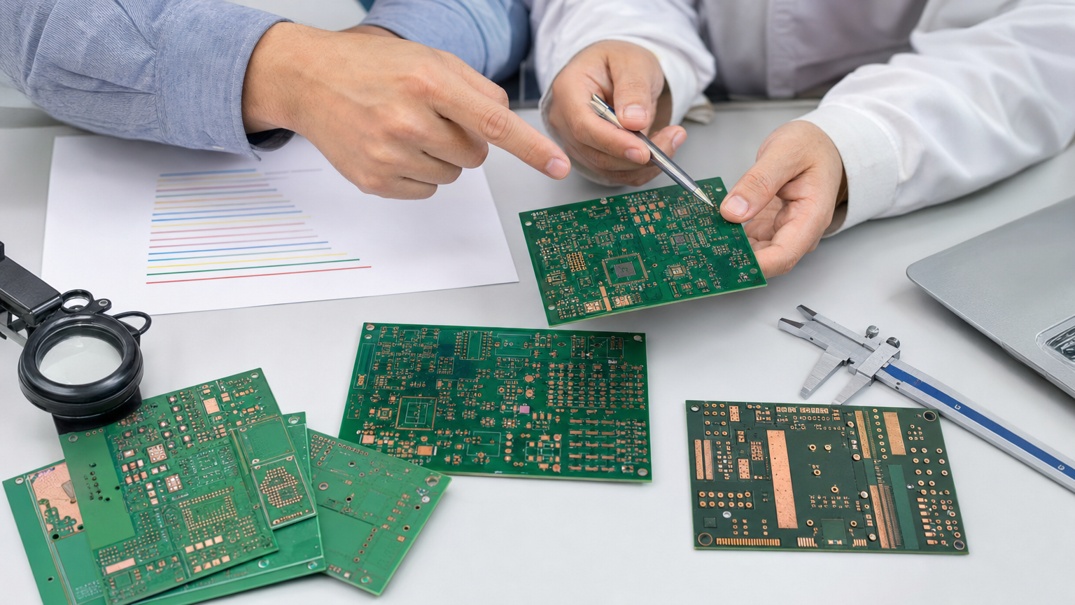
Every blind, buried, and through span listed with start/stop layers.
Copper weights, dielectric targets, and symmetry notes included.
Impedance, backdrill, and critical net classes highlighted.
Coupons, microsection, or special test needs stated in the RFQ.
Blind, buried, or buildup structures, and some high-layer constructions, require multiple press cycles so via spans and registration stay controllable.
High-Tg FR-4 class laminates cover many designs. Lower-loss systems or hybrids appear when serial link loss budgets demand them. Share data rate and length targets.
Impedance targets, backdrill needs, reference layer for each critical net class, and any skew or differential pair constraints that affect stackup.
Send stackup proposal, via map, material list, Gerbers or ODB++, impedance and backdrill notes, quantity, and reliability expectations.
Provide the via map, sequential-lamination intent, laminate preferences, backdrill or impedance notes, quantity, and reliability expectations for CAM review.