More internal routing and plane options
Six layers give engineers room for high-pin-count components, multiple power rails and cleaner separation between noisy and sensitive circuits.
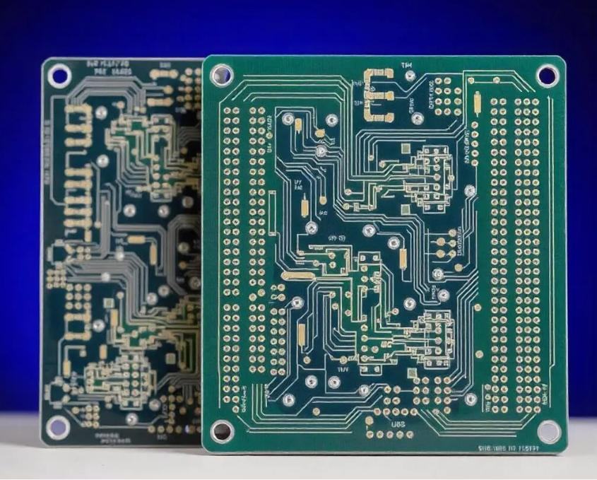
XFPCB China PCB Manufacturer
A 6 layer PCB is chosen when a 4 layer board no longer gives enough routing space, isolation or power-plane flexibility. It is common in industrial controllers, measurement devices, automotive-style electronics, communication modules and compact products using fine-pitch components. XFPCB supports overseas buyers with stackup discussion, DFM review, multilayer fabrication control and practical export quotation support.
Procurement intent
For 6 layer PCB procurement teams, the pain point is usually supplier confidence: can the factory understand the stackup, prevent inner-layer defects and communicate clearly when a design is close to the process window? XFPCB writes each quote around that practical manufacturing conversation.
Six layers give engineers room for high-pin-count components, multiple power rails and cleaner separation between noisy and sensitive circuits.
XFPCB reviews registration, drill-to-inner clearance, lamination balance and copper distribution so fabrication risk is visible before production.
Controlled impedance can be discussed for USB, Ethernet, differential pairs, clock routes and other signals that need consistent geometry.
Material, finish, stackup and test choices are reviewed with both sample and repeat production in mind.
Manufacturing specification
A 6 layer PCB quote should not be treated as a simple board-area calculation. The stackup, copper distribution and testing plan directly affect lead time, yield and long-term product reliability.
| Procurement topic | What to define | Why XFPCB asks |
|---|---|---|
| Layer purpose | Signal, GND, power and split-plane use by layer | Prevents ambiguous CAM decisions and supports better signal return paths. |
| Board material | FR-4 grade, high Tg requirement or special laminate | Industrial and automotive-style products may need stronger thermal and reliability margins. |
| Impedance | Target values and tolerance where needed | Trace geometry depends on dielectric thickness, copper weight and stackup. |
| Drill structure | PTH, slots, via size and BGA fanout requirements | Fine-pitch designs may require tighter review before price and lead time are confirmed. |
| Inspection | Electrical test, AOI and any impedance coupon requirement | Testing expectations should be included early so the quotation is complete. |
Stackup planning
This is a practical starting point, not a locked universal stackup. XFPCB confirms dielectric spacing, copper weight, material and impedance targets against your real files before fabrication.
Application fit
A 6 layer board becomes attractive when the design has multiple power domains, dense connectors, fine-pitch ICs, mixed analog and digital circuits, or controlled-impedance routing that needs better reference planes. The additional layers can reduce compromises that would otherwise make the board harder to test or certify.
XFPCB can help you compare the manufacturing impact of 4, 6 and 8 layer structures. This is useful when the buyer wants the lowest practical cost but cannot sacrifice product reliability.
Manufacturing control
For 6 layer PCB orders, our CAM review focuses on inner-layer clearance, drill registration, plane relief, resin fill risk, copper balance, thermal relief, solder mask clearance and panel stability. These details are not glamorous, but they determine whether the order runs smoothly.
When impedance or high-speed performance matters, the buyer should provide the target impedance, signal layer, reference layer and tolerance. XFPCB can then align the quote with a stackup that is realistic for fabrication rather than a theoretical drawing that is difficult to build.
Order workflow
Procurement teams need predictable communication. The steps below show how XFPCB turns design files into a manufacturing plan that can be quoted, produced and shipped with fewer surprises.
Send Gerber, stackup, drawing, target quantity, impedance needs and material notes.
XFPCB checks the design against multilayer rules and asks practical questions before order release.
Inner layers, lamination, drilling, plating, solder mask, finish and profiling follow the confirmed build notes.
Testing and inspection records are matched to the order before export packaging.
Applications
XFPCB writes each quote around the real product environment, not a generic layer-count label. Tell us where the board will be used so material, finish and testing choices can match the risk level.
FAQ
Industrial control boards, measurement devices, communication modules, automotive-style electronics, dense IoT products and boards using fine-pitch ICs often benefit from 6 layers.
No. Controlled impedance is needed when signal performance requires it. If your design has USB, Ethernet, RF, differential pairs or strict timing, include impedance details in the RFQ.
Yes. If routing density or signal integrity is uncertain, send the project requirements and we can discuss whether 6 or 8 layers is more practical for cost and manufacturability.
Send RFQ to XFPCB
For 6 layer PCB projects, procurement success depends on clear stackup, material and test information. XFPCB can review the files and respond with practical questions quickly.
For a faster engineering reply, include Gerber files, drill files, PCB specification, quantity, delivery country and any impedance, material or assembly requirements.
Related PCB products
Many buyers begin with one layer count and change after DFM review, enclosure checks or cost comparison. These XFPCB pages help you select the most suitable PCB structure before production.