Industry applications

PCBs for Communication Equipment

Communication hardware mixes high-speed digital and RF paths where stackup, impedance and via design decide signal integrity. XFPCB fabricates and assembles communication PCBs with controlled-impedance options and fine-pitch SMT support.

communication PCBRF / high-speedimpedance controllow-loss materialsfine-pitch SMT
PCBs for Communication Equipment at XFPCB
PCBs for Communication Equipment manufacturing support from XFPCB covers material selection, fabrication, assembly options and inspection planning.

Signal Integrity Starts in the Stackup

Antenna modules, baseband boards and optical transceiver companions need consistent dielectric thickness and clean reference planes. Share target impedances, layer count and any Rogers/low-loss material callouts.

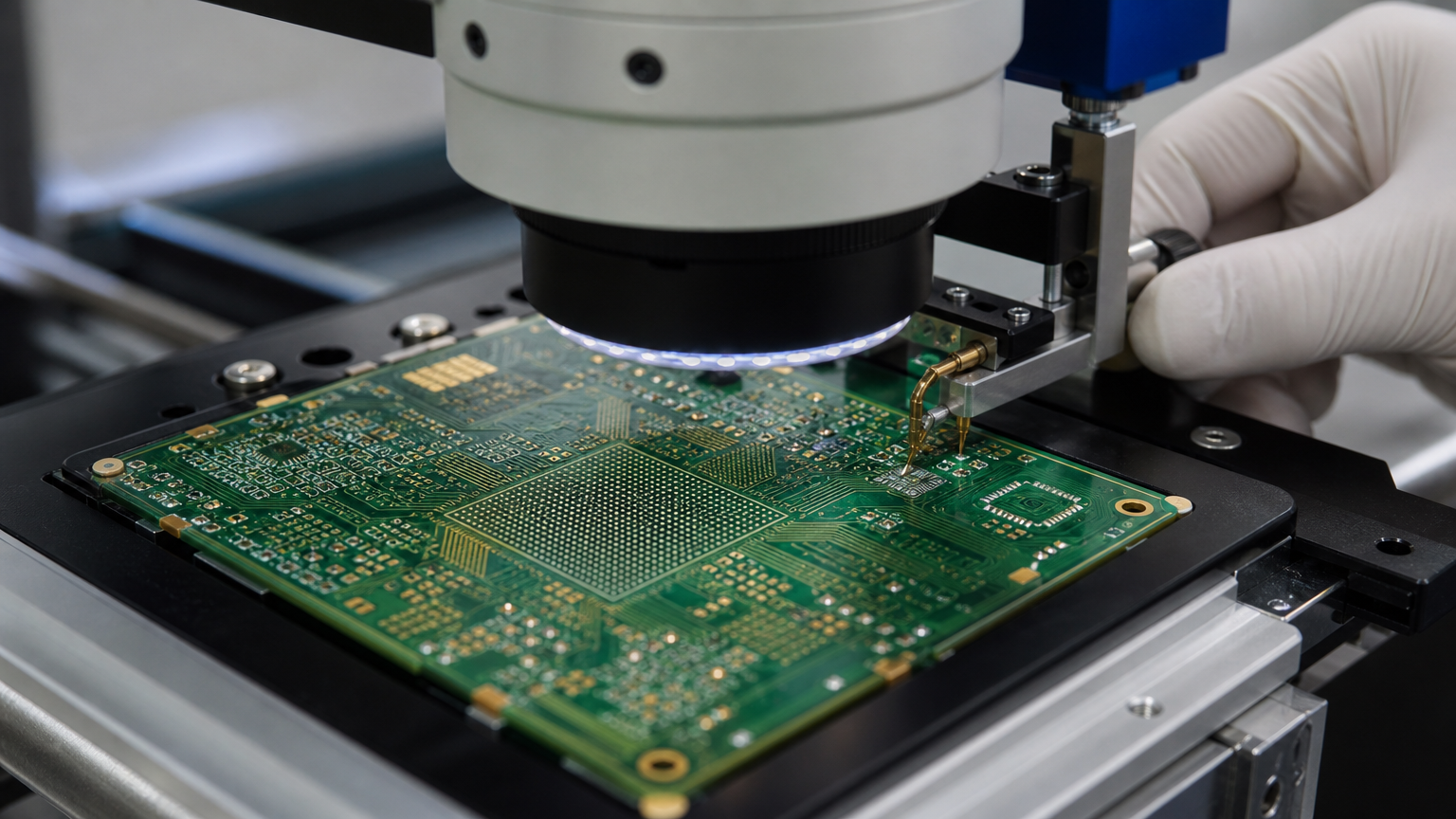
Assembly often includes fine-pitch BGA transceivers - pair this page with our SMT and X-ray resources when packages are dense.

Environment & Electrical Constraints

  • EMI, return-path continuity and thermal rise on PA sections matter.
  • Outdoor radios may need conformal coat and corrosion-resistant finishes.
  • State frequency bands or SERDES rates when they drive material choice.
PCBs for Communication Equipment application review
Application review for PCBs for Communication Equipment connects operating environment to material, finish and assembly choices.

Material & Stackup Considerations

  • FR-4 / High-Tg for many digital boards; low-loss laminates when insertion loss budgets are tight.
  • Impedance-controlled differential pairs with documented stackups.
  • Via structures (through, blind/buried, back-drill) as the design requires.
  • ENIG common for fine-pitch; discuss OSP for cost-sensitive digital only.

Example Use Cases

  • 5G/Wi-Fi access point and CPE boards
  • Baseband and network interface cards
  • RF front-end companion boards
  • Optical module host boards

Why XFPCB for Communication PCBs

  • Impedance-control manufacturing capability
  • HDI options for dense routing
  • SMT assembly for fine-pitch transceivers
  • One vendor for fab + assembly revision control

Communication Quotation Focus

Project AreaXFPCB Guidance
Key inputsImpedance targets, material callouts, layer count
Risk driversStackup mismatch, via stubs, BGA yield
Useful testsImpedance coupons, AOI, X-ray on BGA
Related techHDI, high-frequency, impedance-control pages

Comm DFM Checklist

Impedance Notes

Provide ohms targets and reference layers; we manufacture to the agreed stackup.

RF Material Callouts

Name low-loss laminates when required - do not assume FR-4 substitutes.

BGA Transceiver Plan

Include X-ray expectations for fine-pitch RF/digital BGAs.

Useful Terms

Insertion loss
Signal attenuation along a transmission path.
Back-drill
Removing unused via stub to improve high-speed performance.
SERDES
Serializer/deserializer high-speed links.
Coupon
Test structure for verifying impedance.

PCBs for Communication Equipment FAQs

Can XFPCB hold impedance tolerances?

Yes for controlled-impedance designs when stackup and targets are defined. Coupons can be included when requested on the PO.

Do you process Rogers or other RF laminates?

Discuss named RF materials on the RFQ. Capability depends on the specific laminate and construction.

What assembly risks are common?

Fine-pitch transceiver BGAs and RF connectors - share package drawings and inspection needs.

Prototype RF boards available?

Yes. Start with engineering quantities, lock stackup, then move to volume.

Request a Communication Equipment PCB Quote

Include impedance targets and material callouts with Gerbers for an accurate fab plan.

  • State layer count and impedance requirements.
  • Name any low-loss laminates.
  • Note BGA packages and X-ray needs for PCBA.