More reference planes for high-speed routes
Eight layers make it easier to place critical signals near solid reference planes and reduce crosstalk in compact layouts.
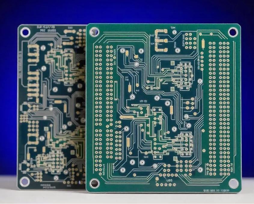
XFPCB China PCB Manufacturer
An 8 layer PCB is selected when routing density, signal integrity, power integrity and component pitch make a lower layer count risky. It is common in telecom hardware, networking equipment, RF modules, high-speed digital products, dense BGA designs and advanced industrial electronics. XFPCB helps procurement and engineering teams turn complex board data into a manufacturable PCB quotation with clear DFM feedback.
Procurement intent
For 8 layer PCB buyers, the real concern is whether the supplier can discuss HDI needs, high-speed routing, material loss, drill structure, controlled impedance and inspection in a way that reduces the risk of a complex order.
Eight layers make it easier to place critical signals near solid reference planes and reduce crosstalk in compact layouts.
Dense BGA escape routing can require advanced via structures. XFPCB reviews these options against cost, yield and lead time before quoting.
At higher frequencies, material choice affects loss and consistency. The RFQ should include speed, frequency and impedance requirements when they matter.
The quote should reflect stackup, drill plan, finish, testing and special acceptance requirements, not only board area.
Manufacturing specification
For an 8 layer PCB, the manufacturing conversation should start with stackup, via structure and material choice. XFPCB reviews these points so the buyer can understand tradeoffs before approving cost and lead time.
| Complexity driver | Common buyer requirement | XFPCB review focus |
|---|---|---|
| High-speed routing | PCIe, Ethernet, USB, DDR, LVDS or other controlled routes | Impedance target, reference plane continuity, trace layer and material behavior. |
| HDI structure | Blind vias, buried vias, microvias or via-in-pad where needed | Sequential lamination, drill feasibility, plating reliability, cost and yield impact. |
| RF or low-loss need | Low Dk/Df material, hybrid stackup or special laminate | Availability, stackup compatibility, price and lead time. |
| BGA escape | Fine pitch packages and dense component placement | Via size, pad design, solder mask, finish and test access. |
| Inspection plan | Electrical test, AOI, X-ray or impedance coupon when required | Define requirements at RFQ stage so acceptance criteria are clear. |
Stackup planning
This is a practical starting point, not a locked universal stackup. XFPCB confirms dielectric spacing, copper weight, material and impedance targets against your real files before fabrication.
High-speed buying
A procurement team may ask for the lowest price, while the design team needs controlled impedance, stable power planes, fine-pitch reliability and low signal loss. XFPCB helps connect those requirements by reviewing the manufacturing data and asking for missing technical details before the quote is locked.
This matters because a small change in via structure, material, copper weight or impedance tolerance can change the cost and lead time significantly. A clear conversation early protects both engineering schedule and purchasing budget.
Manufacturability
Blind vias, buried vias and via-in-pad can solve routing problems, but they are not free features. They add process steps and must be matched to the real need of the layout. XFPCB reviews whether standard through vias are enough, or whether an HDI structure is justified by BGA pitch, board size, layer density or signal requirements.
For high-speed and RF boards, XFPCB can discuss stackup, material and impedance requirements before fabrication. If the design requires special acceptance criteria, include them in the RFQ so the quotation is aligned with the final inspection plan.
Order workflow
Procurement teams need predictable communication. The steps below show how XFPCB turns design files into a manufacturing plan that can be quoted, produced and shipped with fewer surprises.
Provide Gerber, drill, stackup, impedance table, material preference and special notes.
XFPCB checks whether the build structure is practical for fabrication, cost and lead time.
Complex inner layers, lamination, drilling, plating, surface finish and profiling follow confirmed instructions.
Inspection and electrical test are handled according to the accepted order requirements before export packing.
Applications
XFPCB writes each quote around the real product environment, not a generic layer-count label. Tell us where the board will be used so material, finish and testing choices can match the risk level.
FAQ
Choose 8 layers when routing density, signal integrity, power integrity or fine-pitch components make 4 or 6 layers risky or inefficient.
XFPCB can review HDI needs such as blind vias, buried vias and via-in-pad by project. The final process depends on files, stackup, quantity, lead time and acceptance requirements.
Send stackup, impedance targets, material preference, copper weight, via structure, Gerber and drill files, test needs, quantity and delivery country.
Send RFQ to XFPCB
For 8 layer PCB projects, XFPCB needs enough technical detail to review stackup and via decisions before price and lead time are confirmed.
For a faster engineering reply, include Gerber files, drill files, PCB specification, quantity, delivery country and any impedance, material or assembly requirements.
Related PCB products
Many buyers begin with one layer count and change after DFM review, enclosure checks or cost comparison. These XFPCB pages help you select the most suitable PCB structure before production.