Confirm layer purpose before fabrication
A common 4 layer approach uses top signal, inner ground, inner power and bottom signal, but XFPCB confirms the structure against your routing and impedance needs.
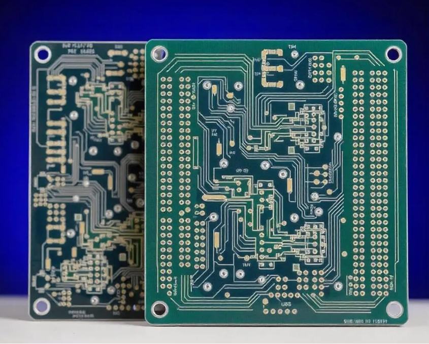
XFPCB China PCB Manufacturer
A 4 layer PCB is often the first serious multilayer step for IoT products, smart devices, wireless modules, compact controllers and commercial electronics. With two outer routing layers and inner reference or power planes, the board can reduce noise, simplify routing and improve assembly density without moving immediately to a high-cost advanced stackup. XFPCB helps buyers confirm the stackup, material, impedance needs and inspection plan before fabrication.
Procurement intent
For 4 layer PCB buyers, the key is not simply adding two layers. The real decision is whether the stackup will support the layout, certification goals, signal paths and production cost of the final product without creating avoidable manufacturing risk.
A common 4 layer approach uses top signal, inner ground, inner power and bottom signal, but XFPCB confirms the structure against your routing and impedance needs.
Solid internal planes can reduce loop area, support cleaner signals and make EMC preparation easier for products moving toward market release.
A 4 layer PCB often provides the best cost-to-performance step for buyers upgrading from 2 layer boards.
Board thickness, dielectric target, copper weight and finish should be discussed early because they affect trace width and impedance.
Manufacturing specification
The exact stackup must be confirmed before production. The example below shows the buying decisions that usually matter most for a 4 layer PCB quote.
| Decision | Typical requirement | XFPCB review focus |
|---|---|---|
| Stackup | Signal / GND / Power / Signal or project-specific alternative | Plane continuity, copper balance, drill structure and manufacturability. |
| Impedance | 50 ohm single-ended, 90 or 100 ohm differential when required | Material, dielectric thickness, copper thickness and trace width must be aligned with the design. |
| Material | Standard FR-4 or high Tg FR-4 depending on reliability needs | Temperature exposure, reflow profile, assembly plan and long-term product use. |
| Surface finish | HASL, ENIG, OSP or project-specific finish | Pad flatness, BGA/fine pitch needs, assembly date and cost target. |
| Testing | Electrical test and visual inspection; impedance coupons when required | Define special test needs in RFQ so cost and lead time are clear. |
Stackup planning
This is a practical starting point, not a locked universal stackup. XFPCB confirms dielectric spacing, copper weight, material and impedance targets against your real files before fabrication.
Engineering fit
A product usually moves to 4 layers when routing on a 2 layer PCB becomes crowded, when a wireless or high-speed interface needs a more stable return path, or when power distribution and ground isolation are becoming difficult. The extra internal planes can improve layout discipline and make the final product easier to debug.
XFPCB works with buyers who need the board manufactured reliably, but also need the quote to make sense commercially. We can review whether your design truly needs 4 layers, or whether the same goal can be met by adjusting the 2 layer design or moving to 6 layers for a denser product.
DFM and quality
For 4 layer PCBs, our CAM review pays attention to layer registration, drill-to-inner clearance, plane openings, resin flow risk, copper balance and solder mask definition. These details affect not only fabrication yield, but also assembly yield and field reliability.
If your board includes USB, Ethernet, RF, WiFi, LVDS or other impedance-sensitive traces, send the target impedance and stackup preference early. XFPCB can discuss practical manufacturing options before your layout is frozen.
Order workflow
Procurement teams need predictable communication. The steps below show how XFPCB turns design files into a manufacturing plan that can be quoted, produced and shipped with fewer surprises.
Confirm layer purpose, board thickness, material, copper weight and any impedance targets.
Review inner clearance, drill rules, plane openings, solder mask and mechanical outline.
Proceed through inner layer imaging, lamination, drilling, plating, outer layer imaging, solder mask, finish and routing.
Electrical test and visual inspection are matched to the order, then boards are packed for export shipment.
Applications
XFPCB writes each quote around the real product environment, not a generic layer-count label. Tell us where the board will be used so material, finish and testing choices can match the risk level.
FAQ
It is better when the design needs cleaner routing, lower noise, more stable power distribution or controlled impedance. For very simple circuits, 2 layers may still be more economical.
Yes. Send your target board thickness, copper weight, impedance requirements and application. XFPCB can review practical stackup options for fabrication.
Yes. If controlled impedance matters, define the target before layout is complete so trace width and dielectric spacing can be matched to a manufacturable stackup.
Send RFQ to XFPCB
A 4 layer PCB quote should include enough engineering detail for stackup and impedance review. This prevents redesign after pricing.
For a faster engineering reply, include Gerber files, drill files, PCB specification, quantity, delivery country and any impedance, material or assembly requirements.
Related PCB products
Many buyers begin with one layer count and change after DFM review, enclosure checks or cost comparison. These XFPCB pages help you select the most suitable PCB structure before production.