

Asking a fab for "good quality FR-4, 1.6 mm, green mask" is not a manufacturing strategy. Circuit board manufacturing is a sequence of chemical, mechanical, and inspection steps where each tolerance stacks on the last. Overseas buyers who understand that sequence ask better questions—and stop comparing quotes that are not actually for the same board.
This is not a factory tour script. It is a map of where yield is won or lost, written for procurement and hardware leads who must RFQ China fabs without becoming process engineers overnight.
Why process literacy beats brochure shopping
Capability pages advertise layer counts, min trace/space, and finish menus. Those numbers matter, but they do not tell you whether your annular ring, aspect ratio, and impedance coupon plan fit the priced process window. Two shops can both claim "0.1 mm trace" while one expects that geometry only on thin outer copper with generous yields and the other will quietly widen features in CAM unless you lock acceptance criteria.
Buyers who can name the stage where their risk lives get better engineering support than buyers who only negotiate price per square centimeter.
End-to-end flow (rigid multilayer mental model)
Use this as a shared vocabulary with CAM engineers. HDI, flex, and metal-core lines insert extra laser, sequential lamination, or dielectric steps, but the rigid multilayer spine still explains most RFQs.
- CAM / DFM gate — netlist compare, spacing, annular ring, acid traps, mask slivers, drill-to-copper
- Inner layers — image, etch, AOI; adhesion promotion (brown oxide or alternatives)
- Lamination — stackup press with registered cores and prepreg
- Drill — mechanical and/or laser; critical for impedance vias and reliability
- Metallization — desmear, electroless copper, panel or pattern plate
- Outer image and etch — final conductors
- Solder mask and legend — dams, openings, cure, registration
- Surface finish — HASL, ENIG, OSP, immersion silver/tin, hard gold, etc.
- Singulation — route, score, or tab-route
- Electrical test and inspection — flying probe or fixture, dimensional checks, final QC
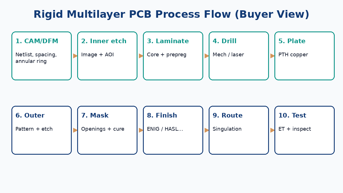
If your board is HDI, ask where laser microvias and sequential lamination sit in this shop's traveler—not a generic textbook. If it is metal-core, thermal dielectric thickness and copper peel become first-class questions. If it is flex/rigid-flex, coverlay, bend, and adhesive/adhesiveless constructions dominate risk.
DFM is not optional paperwork
Short spacing between copper features, insufficient annular ring, hairline mask bridges, and uncontrolled impedance coupons cause real scrap. A competent fab's CAM engineers will flag issues—but only if your files are complete and you answer quickly. Ghosting a DFM questionnaire to "save a day" often spends a week later.
Cost reduction through DFM usually means removing features that force exotic processes—not bullying the shop into ignoring physics. Examples that repeatedly save money without pretending chemistry is optional:
- Convert needless 3 mil / 3 mil outer geometry to a still-dense but standard window when the IC package allows.
- Avoid acid traps and sharp internal acute angles in plane pours.
- Keep non-plated holes and plated holes clearly attributed so drill programs do not guess.
- Provide a real stackup drawing with dielectric targets if impedance is controlled—do not bury Dk hopes in an email thread.
Quote scenarios that look cheap until stage 8
Scenario A — Finish ambiguity. Quote A includes "ENIG." Quote B includes "ENIG" too. Neither states gold thickness. Your BGA assembler expects a thickness window that supports multiple reflows. One fab ships thin gold that works once; the other meets a thicker callout at higher cost. Without the thickness note, you compared stickers, not boards.
Scenario B — Impedance "reference only." Both quotes say controlled impedance. Only one includes coupon design and TDR testing in the price. The cheaper quote modeled impedance in CAM and shipped without coupons. Your SerDes eye looks fine on three boards and fails on the fourth panel—now you are debugging laminate lot variation without data.
Scenario C — Electrical test coverage. At five pieces, flying probe may be included. At five hundred, a fixture might be proposed—or skipped to hit a date. Opens that bare ET would catch become assembly fallout. Ask what is included at this quantity, not what the brochure says is available.
Scenario D — Material equivalence. You specified a mid-Tg or high-Tg laminate family for thermal cycling. The PO confirmation says "equivalent FR-4." Equivalence is not a physical property. Lock named dielectrics when temperature, CAF risk, or impedance depends on them.
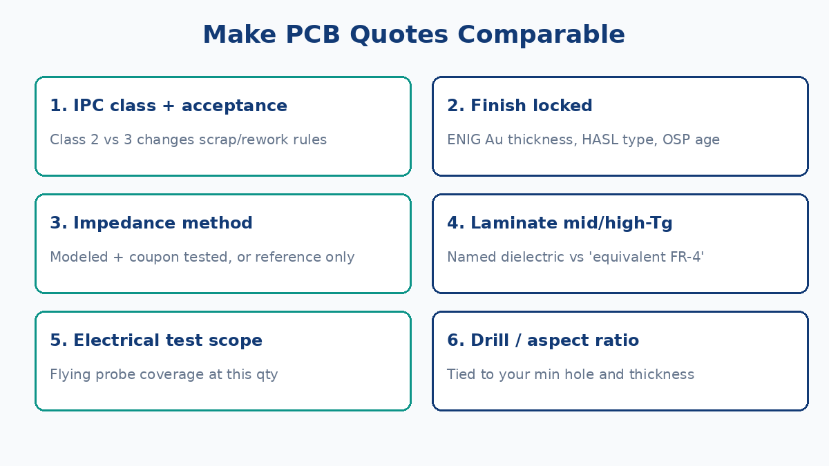
Questions that make quotes comparable
Price spreads between fabs usually come from unspoken defaults: acceptance class, impedance proof, finish thickness, electrical test at quantity, laminate substitution, scrap rules, drill aspect ratio, and whether specials are in the traveler. Lock those items in writing and two quotes become apples-to-apples instead of sticker comparisons.
The buyer FAQ accordion below this article walks through each lock in plain language--what to specify on the RFQ, why it moves cost and lead time, and what a solid overseas fab answer looks like. Use it as your comparable-quote checklist before you tool the first panel.
What "good files" look like before CAM starts
Incomplete packages force fabs to invent defaults. Defaults optimize their traveler, not your product.
A buyer-useful package usually includes:
- Gerbers or ODB++ (and netlist when available) with clear layer mapping
- Fabrication drawing: outline, thickness, tolerances, finish, mask/legend colors, IPC class
- Stackup with copper weights and dielectric targets when impedance or high-Tg matters
- Drill files with plated vs non-plated attribution
- Impedance table when controlled impedance is required
- Panelization notes if you care about array format, tooling holes, or fiducials
- Notes for specials: gold fingers, peelable mask, controlled depth, back-drill maps
If assembly is in scope on the same PO chain, keep fab notes and SMT notes from fighting each other—especially on finish choice (OSP age windows vs ENIG), warpage limits for fine-pitch, and selective gold.

From bare board into assembly without losing the thread
Manufacturing quality includes flatness and finish compatibility with your SMT plan. Boards that pass bare electrical test can still fail assembly if warpage or finish age is ignored. Coordinate fab notes with the assembler early when BGA, fine-pitch QFN, or selective gold is involved.
Concrete example: OSP can be excellent for flat pads and single reflow flows, but it is age- and handling-sensitive. ENIG is often chosen for shelf life and multiple reflows, at different cost and with nickel corrosion failure modes that process control must manage. HASL (lead-free) remains common for through-hole-heavy or cost-sensitive boards, with planarity tradeoffs for fine pitch. Pick the finish for the assembly process, not for habit.
Ionic cleanliness and solderability after storage also sit at the manufacturing–assembly boundary. If boards will sit weeks before SMT, say so. Packaging and finish choice change.
Failure cases worth pricing honesty around
Registration drift on high layer count. Inner clearances that look fine in CAD become annular-ring escapes when lamination and drill stackup tolerances consume the budget. Ask how the shop controls layer-to-layer registration on your thickness and panel size.
Mask slivers and dams. Aggressive copper spacing under mask creates peelable or incomplete dams. That shows up as solder bridges later, which people blame on "assembly" even when fab geometry started the problem.
Over-etched fine traces. Thin copper and aggressive etch compensation can narrow impedance-critical lines. Coupon data and etch process control matter more than a marketing min-trace number.
Via reliability after thermal stress. High aspect ratio holes with thin barrel copper fail in thermal cycling even if room-temperature ET passed. Aspect ratio and plating thickness are buyer questions, not only CAM trivia.
How XFPCB buyers usually shorten the loop
Bring stackup intent, acceptance class, and finish constraints to the first quote—not the third revision. When files are ready, include those notes in the RFQ package and ask XFPCB support to confirm which items are included versus optional adders. Request a quote with Gerbers, stackup, and the question list above so price, lead time, and risk sit on one page.
Buyers who treat manufacturing as a staged physical process stop being surprised by "same board, different quote" outcomes. The board did not change. The assumptions did—and assumptions are something you can write down.