
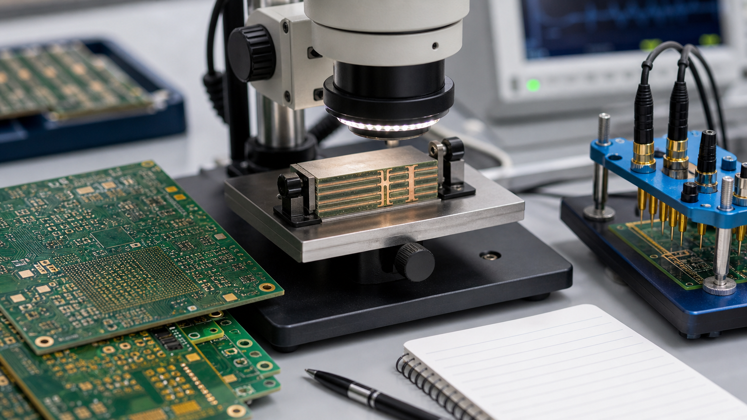
GPU baseboards and accelerator cards inside AI servers look like "just another multilayer" until registration, low-loss lamination, back-drill, and large-BGA flatness show up on the same traveler. Schedules slip when architecture adds layers while purchasing still expects FR-4-era lead times.
An AI server PCB interconnects CPUs, GPUs or accelerators, HBM/DDR, PCIe, high-speed fabric links, NICs, and dense power stages under higher thermal and current stress than a conventional server motherboard. Manufacturing risk stacks: high layer counts, HDI escapes, hybrid low-loss materials, via-in-pad, and impedance windows that leave little CAM forgiveness.
Boards inside the system
Not every board in the rack carries the same difficulty. GPU substrates and OAM/accelerator cards push fine interconnect and HDI. GPU baseboards / UBB designs often combine the hardest routing density, power delivery, and thermal constraints. CPU motherboards still need DDR and PCIe discipline. NIC cards live or die on SerDes channel quality. Power boards need copper weight and thermal paths that match transient current.
Quote and DFM conversations should name which board you are buying. A "server PCB" RFQ that mixes NIC loss budgets with power-board copper without saying so produces useless price comparisons.
Why layer count and HDI appear together
Routing escapes around fine-pitch BGAs, separating high-speed pairs from noisy power, and keeping reference planes continuous usually force 16-32+ layers on aggressive platforms. Layer count alone does not fix SI: stackup still needs controlled dielectric heights, copper balance against warpage, and materials matched to channel loss.
HDI (microvias, blind/buried structures, sequential lamination) shortens escapes and raises density when through-hole dog-bones no longer fit. It also tightens registration, plating, and via reliability requirements - budget NRE and yield risk accordingly.
Materials, impedance, and stubs
Critical SerDes, PCIe Gen5/6-class, and fabric channels often need low-loss or ultra-low-loss laminates and smoother foils on selected layers. Hybrid stackups keep cost sane by reserving premium materials for loss-critical strata.
Controlled impedance must be written as targets plus test method, not a slogan. Back-drill maps with residual stub limits belong in fab notes before tape-out; discovering stub resonance after mechanical freeze is expensive. Via-in-pad for fine BGAs needs fill, plate, and planarization quality that assembly can solder.
Power, flatness, and assembly
Accelerators create fast current steps. Plane strategy, via inductance, copper weight, and decoupling placement are manufacturing-relevant because they drive layer count and warpage. Large BGAs on thick boards need flatness compatible with reflow; fixtures, profile work, and X-ray inspection are part of yield, not optional extras.
SPI, AOI, and X-ray should cover the packages you actually place. First-article plans should include impedance coupons correlated to the production stackup.
Yield risks to price in early
Registration stackup on high layer counts, impedance drift from dielectric or etch variation, CAF risk on aggressive constructions, microvia reliability, and warpage under large packages dominate scrap stories. Panelization and prototype-to-volume correlation reduce surprises.
Share stackup, impedance tables, back-drill maps, and BGA pitch with the fab early. Related reading: HDI PCB, multilayer PCB, and server and data storage PCBs. Submit packages via how to place an order.