
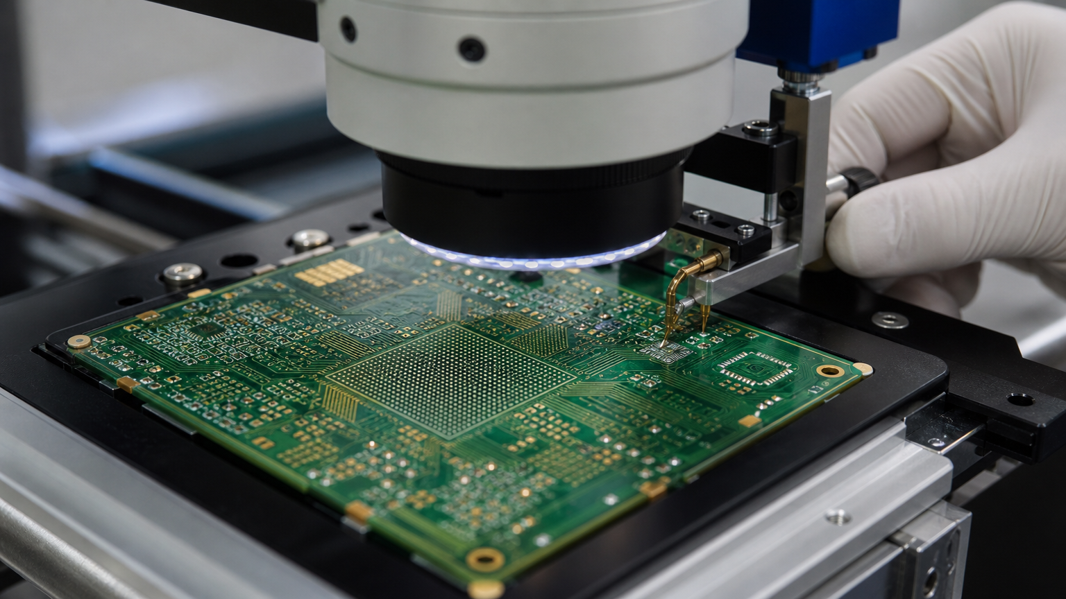
BGA and CSP packages moved high pin-count silicon off the package perimeter and onto the bottom face of the component. That shift is why modern processors, memory, and ASICs fit into products that QFP-era layouts could not. It is also why SMT yield now depends on via strategy, paste volume, flatness, and X-ray criteria instead of a quick visual glance at gull-wing toes.
Overseas engineering and procurement teams often treat BGA and CSP as synonyms. They share area-array ideas, but they optimize different goals.
What a BGA is solving
A ball grid array places solder balls under the package as both electrical and mechanical connections. Instead of crowding hundreds of leads around four edges, the array uses the package footprint more efficiently. For the same I/O count, board area can drop dramatically compared with fine-pitch QFP.
Practical advantages include higher I/O in a given outline, more workable ball pitches than equivalent edge-lead crowding, self-alignment from solder surface tension during reflow, and shorter interconnect paths that help high-speed behavior. None of that removes process control: pad design, mask openings, coplanarity, paste printing, placement accuracy, and reflow profile still decide joint quality.
Common families include ceramic BGA (CBGA) for tougher thermal and reliability needs, plastic BGA (PBGA) for volume commercial use, and micro-BGA / uBGA with finer pitches for compact products. Pitch might sit near 1.27 mm or 1.0 mm on mainstream devices and drop toward 0.8 mm, 0.65 mm, 0.5 mm, and below on miniaturized parts. Finer pitch quickly pulls in HDI, via-in-pad, tighter SPI, and stricter inspection.
What CSP pushes further
Chip scale package forms keep the finished package close to the bare die outline. Rules of thumb used in industry discussions put package side length near the die and package area only modestly larger than die area. The point is miniaturization and short paths, not only "more balls."
CSP structures can support very high connection counts in a tiny outline, lower interconnect parasitics, and in some constructions a short thermal path to a heat spreader. They show up in portable electronics, memory modules, and dense consumer and networking products where every square millimeter matters.
BGA versus CSP in plain terms
BGA is the workhorse answer to high I/O density with a manageable area-array SMT flow. CSP is the next step when package size must hug the die and electrical length must shrink further. Both hide joints under the body. Both punish vague land patterns and "AOI only" quality plans.
Assembly and inspection realities
Because joints are invisible from above, X-ray is the normal way to look for voids, opens, bridges, and misalignment after reflow. Pad design and solder-mask-defined versus non-solder-mask-defined choices shape the joint. Unfilled vias under balls can wick solder and starve joints. Warpage on thin packages or large boards creates open corners that electrical test may catch late and optical inspection may miss entirely.
Put pitch, ball map, via-in-pad fill/cap requirements, flatness expectations, paste/SPI plans, and X-ray void criteria on the same note set as the land patterns. Underfill is a product decision, not an afterthought when first articles show mechanical weakness.
For manufacturing, align BGA PCB manufacturing capability with any HDI PCB needs the escape routing forces, and require X-ray inspection in the PCBA plan whenever area-array packages are on the BOM. That combination is how dense BGA and CSP builds move from hopeful prototypes to repeatable production.