

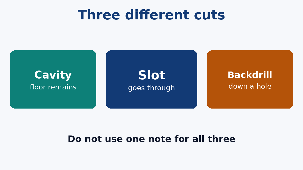
A cavity is a pocket. It has walls and a floor, cut to a controlled depth from one side of a board that is already pressed. A slot has no floor. A backdrill is a round bit sent down a plated hole to cut away barrel copper that a signal is not using. The three notes get copied onto each other, and the shop then has to guess which feature you bought.
What the cutter is doing
After lamination the layers are where the press left them, not where the CAD stackup drew them. An instruction that only says "mill to layer 3" asks the machine to find a copper sheet whose height moved with the prepreg. Sometimes the tool stops in dielectric above that layer. Sometimes it kisses the copper. Sometimes it goes through it. None of those is a depth.
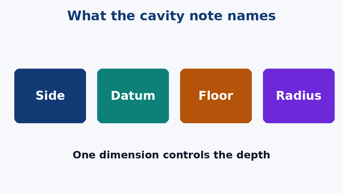
Give the pocket a datum and one controlling dimension. The datum is a real surface: the finished top, or the finished bottom, named as such. The controlling dimension is either the depth down from that surface or the thickness of board you still want under the floor. The other number can be on the drawing as a reference. If both are toleranced as if they were independent, they will disagree as soon as the panel is a little thicker or thinner than nominal, and the shop has to break one of them.
As an illustration only: a 1.6 mm board with a 1.2 mm pocket leaves 0.4 mm under the floor before any variation. That 0.4 mm is the whole margin against cutting through. It is not a specification, and it is not a promise that 0.4 mm is enough for your stack. It is why "as deep as possible" is how pockets become slots.
Which side the tool enters is part of the note. A pocket from the bottom does not show on the top assembly view, and it still cuts whatever copper is in the way. Top and bottom pockets that overlap in X-Y are a remaining web in the middle. Say so, or the two programs will meet.
The floor is a requirement, not a texture
Two floors are common, and they are different products.
Dielectric left. The floor is resin and glass, no copper showing. That is a clearance pocket: a tall part, a connector body, a lid that needs the board locally thinner. Tool marks in the resin are normal unless you have a cosmetic reason to forbid them. The risk is breaking through, or scuffing a copper layer you meant to leave buried. A keep-out on that buried layer, measured from the finished wall after the cutter's wander, is what protects it. The CAD outline is smaller than the zone the tool can touch.
Copper exposed. The floor is a named layer, brought to the surface on purpose: a contact, a shield seat, a plane you intend to bond to. That copper is now an outer surface. It can short to the part you drop in the pocket. It needs a finish if it must be solderable, and it must not get a finish if the note said bare. "Expose layer 3" without saying whether that copper may be scratched, plated or soldermasked is three different floors.
Wall plating is a separate switch. Plating the walls connects the floor copper to whatever those walls cut through. Leave it off unless that connection is the point. A clearance pocket with plated walls is a short waiting for a metal housing.
Inside corners are round. The tool is an end mill. A square internal corner in the CAD will be cut to the tool's radius, or the job will stop for a question. Draw a radius the cutter can make, and keep parts and copper out of the crescent the tool cannot reach.
Not a backdrill, and not a coin seat
Backdrilling removes unused plating from a hole that already goes through the board. The thing you specify there is the must-not-cut layer and how much stub may remain. The tool is sized to the barrel, not to a pocket outline. A depth-rout pocket does not remove a via stub, and a backdrill note does not recess a component. If both are on the same board, they are two programs, two drawings, two checks.
A pocket machined to fit a metal insert, such as a copper coin, is a third feature again. The floor and the walls have to match a piece of metal, not just clear a component body. Clearance, press fit and how that metal joins the copper are their own drawing. Do not take the component-cavity note in this article and reuse it as an insert drawing.
How you know the pocket is the one you drew
A continuity test will not measure depth. It might notice a short if the cutter hit a plane and the net is in the fixture. It will not notice a floor that is 0.2 mm thin, or a corner that ate a trace which was not on a tested net. The check is mechanical: depth from the named datum, remaining thickness if that was the controlling number, and a look at whether copper is showing where the note forbids it. Do that on a coupon or on the first board of the lot, per pocket program. One pocket from the top does not prove a different pocket from the bottom.
Our Manufacturing Files page is the Gerber, drill and drawing set a quote is built from. The pocket outline has to be in that set as a rout path, on a mechanical layer the shop will cut, not only as a keep-out in the layout and not only as a sentence in a PDF. A keep-out tells the designer to stay clear. It does not start the spindle.
The note, without a fake tolerance
- Side of entry.
- Outline layer that is actually routed.
- Datum surface, and one controlling dimension: depth or remaining thickness. The other marked reference.
- Floor: dielectric only, or a named copper layer exposed. Wall plating yes or no. Tool marks allowed or not, if you care.
- Copper keep-out from the finished wall, not from the ideal CAD line.
- Internal corner radius the tool can cut.
- That this program is not the backdrill program and not an insert fit, unless you have a separate note for those.
Depth is a number from a surface you can measure. "To layer 3" is a wish about where the copper ended up.